


JINSUNG Electronics is a manufacturer specialized in SMT and produces and supplies PCB, PCB which is key components of display such as TV, monitor and etc.
PROJECT
ABOUT PROJECT
SMT Manufacture
HOME - ABOUT PROJECT - SMT Manufacture
SMT Manufacture
JINSUNG Electronics is a manufacturer specialized in SMT and produces and supplies PCB, PCB which is key components of display such as TV, monitor and etc.
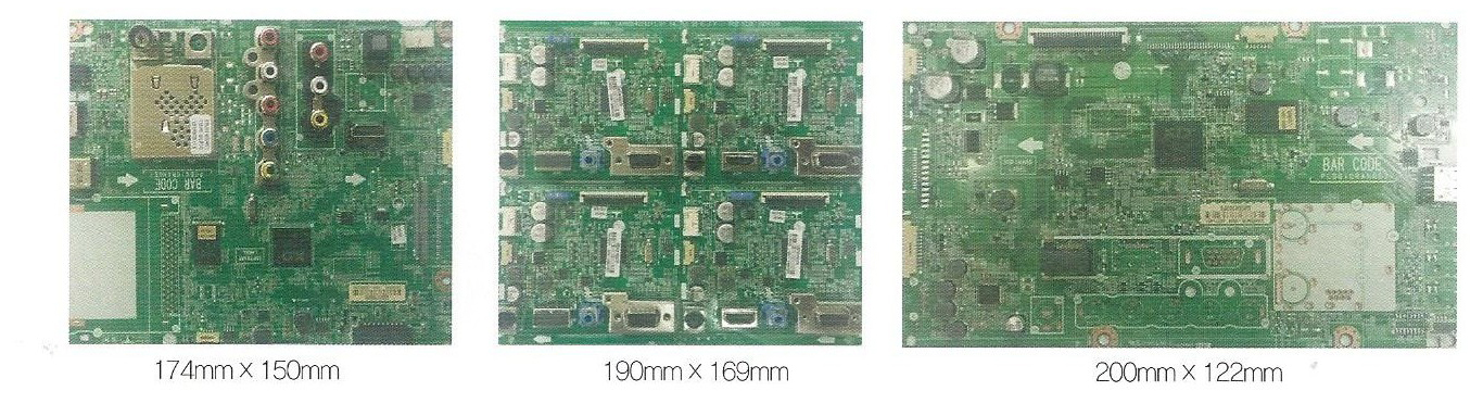
1. SINGLE PRINTED CIRCUIT BOARD (Small, medium and large size in PCB)
SMT is a technology to mount various mounting parts on printed circuit board (PCB)
Air cleaned Bare PCB is processed to (Pb free) soldering in screen printer and sequentially surface-mounted with more than 600 ~2,000 parts by Auto Teaching Instruction of MOUNTER. And then, the PCB goes to next process of REFLOW and AOI in sequence.
2. DOUBLE SURFACE PRINTED CIRCUIT BOARD (Small, medium and large size in PCB)
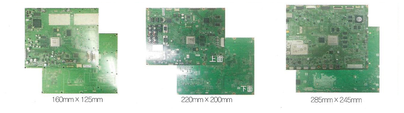
PCB(Top surface) SMT production means that Bare PCB is soldered and mounted with more than 600~2,000 patrs and the electrical bonding between PCB's surfarce and the mounted components is made during REFLOW process.
PCB(Bottom) SMT production means that the(Top) PCB having a SMT(I) process is soldered and mounted again after upside down.
Inspection
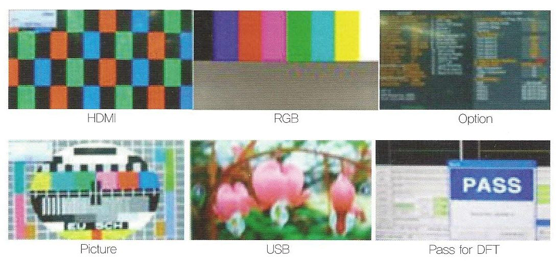
1. DFT(Digital Function Test)
Digital Function Test (DFT) performs the performance test on TV and monitor PCB/PCBA
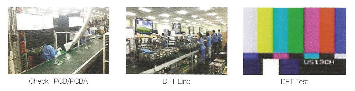
PCB/PCBA for TV and monitor is tested for electrical conduction, video, voice, color and other functions in accordance with customer specification
2. SMT INSPECTION
PCB/PCB produced by SMT will go through inspection process as below.
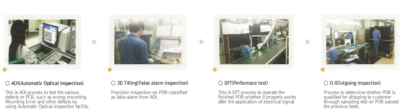
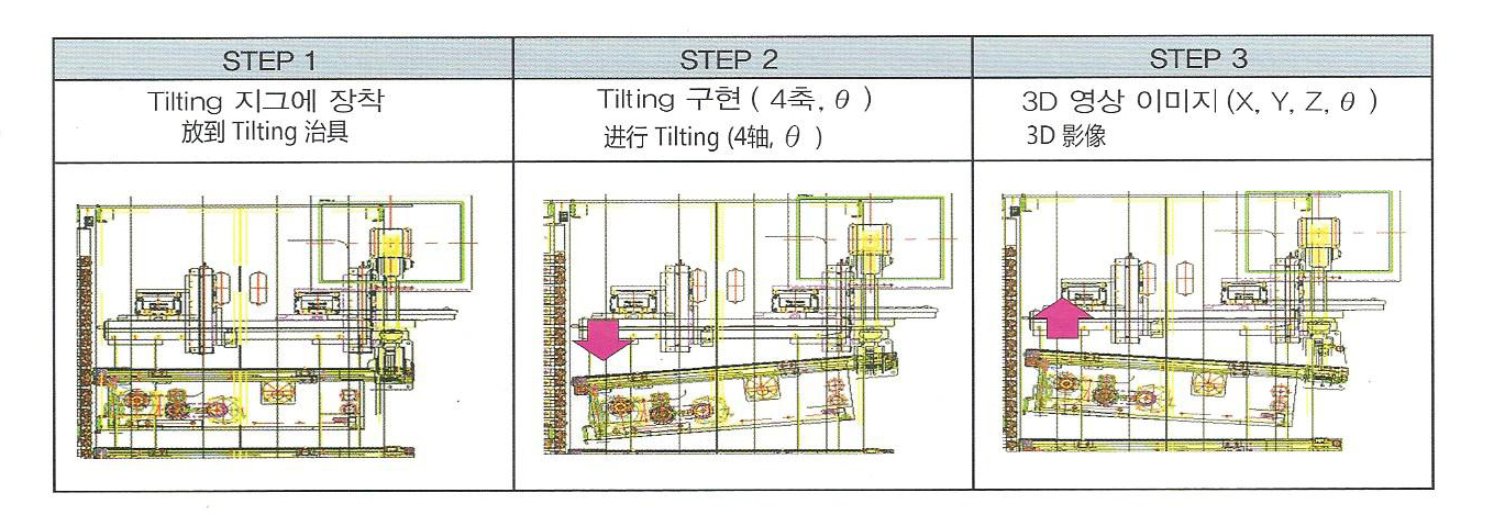
3. INSPECTION TECHNIQUE FOR PCB WITH FALSE ALARM
False alarm and tilt type visual inspection
False alarm from 2D AOI (Automatic optical tester) is mostly test error of AOI device and 100% of these PCB with false alarm also go through precision inspection ( by Tilting type 3D monitoring inspection).
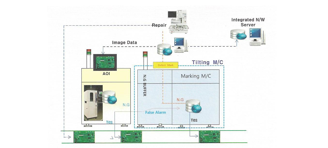
Inspection Process
The PCBs rated as false alarm from 2D AOI go to be mounted on NG BUFFER sequentially.
PCBs automatically pulled out from NG BUFFER is monitored after tilting toward Z-axis and taken visual images.
Perform monitoring inspection on 3D visual images of upper, side and lower side of PCB by inspector.
PCBs passed the 3D precision test are forwarded to In-line and those which failed to pass will be remounted on NG BUFFER as sequence.
Defect location of PCB is automatically marked (Defect Location Numbering) to the PCB which is finally failed in quality.
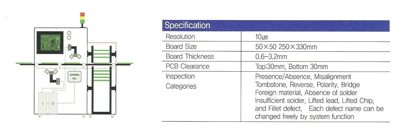
4. DOUBLE SURFACE AOI INSPECTION
Double surface inspection device for PCB
Inspect double surfaces of PCB/PCBA at the same time
Suitable for test after the final SMT process
Optimized for PCB/PCBA by high resolution and high speed scanning technology
Provides objectivity and reliability in the mounted surface of PCB
Line Scan Camera
Image capture device consists of camera and optical part which converts an optical axis to horizontal axis.
Line scan camera scans each line of PCB interoperating with encoder of Servo- motor.
Coaxial Box Lights
Coaxial Box Lights is that optical axis from lighting device is located in same axis with the reflected light coming into camera
Lights consist of various lighting systems in order to perform inspection on false alarm or bird caging.
Mutual : JINSUNG ElectronicsCEO : Gil-ho Seo Address : 359 4 Gongdan-ro (Geumjeong-dong) Gumi-si, Korea 730-410
Business : 511 - 81 - 04714 TEL : 070 - 8228 - 4263 FAX : 054)971-8180
COPYRIGHT ⓒJINSUNG Electronics COMPANY. ALL RIGHTS RESERVED